What is FM demodulator. IC type FM demodulator explained. CA3089

What is FM demodulator. IC type FM demodulator explained. CA3089

Description of FM de-modulator CA3089

Here in this article we will explore the block diagram of IC CA3089 which is commonly used as FM demodulator. This diagram can be available from IC CA3089 datasheet. The block diagram shows that the incoming signal is passed through three amplifier stages. All three amplifier stages have its own lever detectors. The output of these three amplifiers are summed together and fed through pin 13. Here the signal level can be measured. When the signal level enters the limiting the current of the signal reaches its maximum value.

CA3089 FM demodulator IC block diagram


Output stage of FM demodulator

Output of the final amplifier is fed to quadrature detector stage which convert frequency deviation or frequency changes to the amplitude changes. This is there actual demodulation of FM signal into audio signal or base frequency information. How this demodulator works is shown in the bellow image.

FM demodulator function diagram


Here shown the RLC network which is formed of two capacitors, one inductor and two internal resistors. The capacitors and inductor are outside the chip or they are external components. This RLC network is providing a 90 degrees phase shift at intermediate frequency or IF. From here the 10.7Mhz signal and the original siganal are fed to the mixer stage where the phase of the signal is detected and voltage is produced which is proportional to the phase shift or phase difference.

FM demodulator output response on frequency band

The response of this demodulatior is nonlinear over the large frequency band. Anyhow on narrow band its frequency response is nearly linear. It provides very low signal distortion of 0.1%. The value of signal distortion is dependent of circuit design and circuit calibration. If realistically designed, the circuit performs very well with very low distortion. This type of circuit is very suiatable for such small applications as it is very stable and consuming very low power and providing great degree of simplicity. Also its price is low too.

Due to all these benefits and qualities the CA3089 is the better choice for many portable FM radio receivers.

Continue reading

What is Frequency Modulation FM. FM explained

FM or frequency modulation is a mean of modulating carrier with information or base signal in radio technology so that the RF or radio frequency can be propagated to distance receiver from a transmitter. There are three basic methods of modulation for radio frequency. They are CW or continuous wave, AM or amplitude modulation and FM or frequency modulation. CW or continuous wave was used in older days for Morse code transmission in the way that a fixed frequency and fixed amplitude signal wave was switched on and off and transmitted. this on and off signal was carrying Morse code information to the other side of receiver. In amplitude modulation a fixed frequency wave is used whose amplitude is varied according to the base frequency or information. Or in other words the base information is overlay of the carrier frequency signal. The next type is FM or frequency modulation in which the amplitude of the carrier signal is kept fixed and the base information is used to change the frequency of the carrier signal to take the information.

Different methods of modulation

The time of CW had passed. There in no more use of Morse anywhere. But still the amplitude modulation and frequency modulation is in use. Amplitude modulation are affected much from external disturbances where the FM or frequency modulation is affected very less. This is the reason we hear very clear ad beautiful music and voice at FM whereas at AM band this is not possible. The other reason for clarity is the frequency modulated signal provides much wider band for modulation of base signal or information which is up to 75Khz whereas the AM or amplitude modulation provides only 5Khz of bandwidth. Modren days FM or frequency modulation signal can even modulate stereo audio signal as base frequency which can be received by a stereo receiver are receiving end. Sure stereo audio signal is way better and natural compared to mono audio signal.

Frequency modulation can also use the concept of pre-emphasis and de-emphasis. In this system the FM signal is much more amplified at transmitting end and is then attenuated with the same ratio at receiving end. In this method the unwanted signals injection is also reduced and we receive a very clear signal at receiving end.

Modern days FM receivers are using one single chip IC which is responsible for doing all the required tasks and functions. Receivers are comparatively simple for FM. FM is using high frequency band and that frequency the need of the antenna is less. A small size antenna can effectively transmit and can receive the signal. One disadvantage of FM is the signal is highly direction or it uses line of sight. In normal conditions the transmission limit is 25Km circle for an FM signal.

Continue reading

Supper FM 9 radio receiver block diagram and features

 Here in this article you will see the block diagram and feature of a high quality FM radio receiver. FM radio receivers are very popular these days due to FM broadcast available all over. A good quality FM radio receiver is capable of producing quality audio which had been broadcast at the time of transmission. The receiver should be capable of receiving and producing stereo FM signal. This FM radio receiver is battery powered and is portable because it can be powered from a single 9V battery. A PP3 battery could do or a rechargeable battery could also work just fine. The power consumption of this radio is just moderate and battery could last for a few hours of listening. Dual power option is available if somewhere power line is available, the best choice to operate this radio could be the means power.

Supper FM 9 block diagram

This Supper FM 9 radio receiver circuit is based on superheterodyne function. In superheterodyne design the radio signal is amplified and is fed back again in the input several times. This way the signal become very strong and very large to be better identified by the audio frequency stage. The signal from the antenna is fed to the band bass filter. Then this signal is few to the tuned RF amplifier where the channel selection is made and a particular frequency band is selected to output. The band selection is made by a varicap diode whose capacitance can be varied by applying reverse biasing of the diode. Such diodes are very common in modern tuning circuits where a voltage signal is used to make the tuning. There are common in digital type tuning circuits.

Next is the mixer stage where the signal is mixed with the local frequency oscillator frequency to obtain the difference of the two frequencies which would be exact 10.7MHz. Then the signal is fed to the next stage 10.7MHz band pass filter where any other unwanted signals are rejected and the desired 10.7MHz signal is fed to the next stage the IF amplifier stage. In IF amplifier stage the signal is amplified. 

Next this signal is fed to the limiter and demodulator stage where the signal is seperated from the carrier. When the signal is separated from the carrier, the carrier is rejected and the only audio signal is few to the audio amplifier stage. Before sending the signal to the audio amplifier stage, the signal is fed to another stage the stereo signal detection where the signal is divided into two audio signals, L and R stereo signals. Then these L and R stereo signals are fed to two separate audio amplifiers where both L and R signals are amplifier to the the level so that two speakers could be driven by this audio signal.

Continue reading

TP4056 li-ion 3.7v battery 18650 Charging Module Detail, Pinout and datasheet


 In this text I will discuss about the famous TP4056 charging module which is a 3.70V  Li-ion battery 18650 in detail. The pinout, characteristics, setup and calibration for battery value will be covered in this text. TP4056 charger module is a very tiny size module to charge li ion batteries that it can fit anywhere inside any electronic equipment or instrument. TP4056 module consists of a single chip IC TP5640  and a few other supporting components which makes high quality and precision charging module which gives complete solution to automatically charge li-ion batteries of any small size. Using TP4056 module to charge the li-ion battery, it provides full battery life and effective charging to prolong battery life with great efficiency. Using TP4056 battery charging module you can make the line powered equipment less power consuming and the old equipment using dry cell can be converted to rechargeable battery solution.

TP4056 Charger or charging module

TP4056 Charging Module Characteristic and Technical details

  1. Input mini usb, micro usb and C port as well as soldering pad connections
  2. Two indication for charging status.
  3. Over current and over charging protection
  4. Battery charging current can be adjustable or can be controlled by replacing one resistor value to certain value which could be obtained easily from the table bellow in this text.
  5. The module can connected to AC DC power supply by a usb type cable
  6. Battery temperature measurement is made by IC. It will prevent during overheating.
  7. Cheap in price and easily available everywhere
  8. Softly starts charging. Soft start charging feature.
  9. Automatic cut off charging when battery fully charged.
  10. Battery full charge indication
  11. Battery charging current can be adjusted from 130mA to 1000mA.
  12. wide power supply voltage range form 5.0V to 10.1V DC.

TP4056 charger module explained

TP4056 charging module is a complete charging solution which provides efficient charging solution to 3.7V single rechargeable cell. This module can be used to charge any small size 3.7V lithium iron battery including 18650 cell. This charging module name employees TP4056 due to TP4056 chip used inside this module which is the main part of this module. A few external components are used to support the chip.

The IC has a temperature sensing pin where an NTC can be connected which would be placed on the battery and that NTC will stop charging when the battery under charge temperature will get increase. There are two led indicator sink type pins on the chip in which on of the LED shows the charging state and the other led turns on when charging is complete and charging is disconnected and the charged led would flesh.

TP4056 provides steady 1A charging current which could be reduced or programmed by replacing the value of one resistor.

Continue reading

Supper capacitor or suppercapacitor

 Energy storage device

Super cap

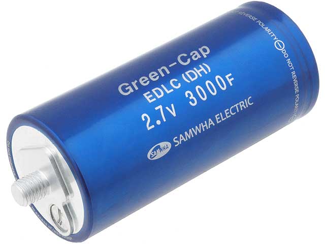
The supper capacitor or super cap is same like other electrolytic capacitors but they have a very big capacity to store large amount of charge. Most commonly used capacitors in audio amplifiers and stereos have values like 220UF, 500UF and 1000UF. UF stand for micro farads. In radio frequency circuits very small capacitance capacitors are used for example 10 pf or less. They are very small capacitors. In power supplies one can see large size capacitors like 1000UF to 10000UF to reduce the power supply ripple. There are hundreds and thousands of capacitors are used in any kind of electronic equipment. These capacitors have specific capacitance and voltage rating. Same is true for super cap. super cap have both capacity value as well as voltage value. The capacity is very very high for supper capacitor like in few hundred and even thousands Farads and the voltage rating is very low like 2.5 Volts for each super cap. Supper capacitor has quality that they can be charged very fast and they are capable of providing very large current peak. Also they don't tendency to degrade with passage of time like regular batteries.

Super cap or supercapacitor


Charging super cap

Super cap can be charged very quickly and they have ability to discharge very quickly too. They can be used as regular batteries with solar system, in electric vehicles, in torch lights and many other applications where batteries had used.

Super cap
Super cap

Supper capacitors don't emit gas like lead acid batteries but they do store charge less than lead acid batteries. Supper capacitors can be used in series to increase the applied voltage or in parallel to increase the storage capacity. Hence strings of series are made and these strings are connected in parallel together to make reasonable battery having accepted voltage rating and charge store capability.

Super cap in series and parallel strings

Super cap charger

Supper capacitors could be charged using a DC to DC boost converter. But current limitation is a must for charging supper caps. Supper cap acts like a dead short if connected to a power supply for charging. It would cause to blow the power supply fuse or it would burn the power supply if the power supply have no over current protection.


Continue reading

TP4056 Lithium ion Lithium iron Battery Charge Controller

TP4056 is a Lithium iron rechargeable battery charge controller IC. The TP4056 IC is providing full constant voltage and constant current characteristics for charging a single 3.7 volt Lithium cell or battery. The TL4056 is ideal chip to do the function. It's charging rate or charging current could be controlled by external resistor on program pin. It has both charging and charge complete sink type input pins where two different color LEDs could be connected to show the status of the chip. The TP4056 IC comes in SOP package and it needs very few external component to function. The less external components and its small size makes it ideal and the best choice to be used in portable applications.

TL4056 IC typical charger circuit

TP4056 can be used in usb applications wall mounted power packs. tp4056 don't need a blocking diode to prevent battery reverse current flow due to internal chip mosfet arrangement. tp4056 has internal thermal protection which prevents chip during high current and high temperature operation or in high ambient temperature. tp4056 output charging voltage at battery terminals are fixed to 4.21V or 4.2 volts. The current rate could be set by a single external resistor. When the charging current reaches to 1/10th of the charging current, the chips stops charging it disconnects battery from charging source. For monitoring two status LED are provides which shows the charging state.

TL4056 or TP4056 charger arrangement
tl4056 ic current programming resistance selection could be done using the following table bellow.
TL4056 IC program current setting resistance values.


The maximum charging current of the tl4056 chip could be programmed 1000mA or 1A linear. There is no need of external mosfet to charge the battery. The internal mosfet inside the chip is enough to accomplish the job. Tl4056 input voltage range is from -0.3V to 10V. TL4056 maximum junction temperature is 144℃ and the working temperature is -40 ℃~85℃

TP4056 SOP pakage

TL4056 charge controller is widely used in digital camera, usb powered chargers, torch lights, battery operated toys, cellphones, cordless telephones, pda, GPS devices, portable devices, charging stations, stroboscope, digital oscilloscope battery powered, multimeters with chargeable batteries and many more.

Continue reading

RM6204 Switching regulation smps power management IC


Here in this article we will discuss a small SMPS current mode smps power management IC. RM6204 is a beautiful smps power management IC which is very commonly used in small size smps power supplies and cell phone chargers. RM6204 is a 12W and line voltage regulator IC which is a simple to use and simple to construct single chip smps controller. RM6204 is official IC for Huawei cell phones chargers. This IC RM6204 needs very few external components to function. The power of the smps is limited trough external components like chopper transformer and other resistors and capacitors values. This IC internal switching transistor has capability to withstand 700 volts. The switching transistor can switch 800mA current continues. The overall IC power dissipation is 1000 mW or 1 Watt.

RM6204 SMPS Regulator circuit
RM6204 SMPS regulator power supply circuit schematic


Above is the circuit schematic for RM6204 smps regulator power supply. Such power supplies are small and suitable for small power needs like cellphone chargers and toys battery chargers. They are capable of providing steady 12 Watts of power. The above circuit is straight forward power supply circuit with feedback loop control. The feed back is observing the output of the circuit and continuously controls the input side PWM signal to regulate the output of the power supply regardless of input voltage changes and output load changes within certain limits. The feedback components are U2, IC3, C20, C6, R8, R9, R10 and R11. These all components makes a feedback loop which regulates the output of the power supply.

RM6204 SMPS controller IC pin connections detail

The above diagram shows the pin connection detail for IC RM6204 smps controller. This IC has 8 pin DIP package. It's available in hole through design.


Here is the internal block diagram of RM6204 IC. RM6204 IC is manufactured by Reactor-Micro semiconductor company.


RM6204 IC block diagram

Here below is RM6204 smps power supply image. This is image for one cellphone charger. You can see only the top side of the power supply board here. Where is this board is smd technology and there are components mounted on the back of the pcb also.


RM6203 IC smps power supply


Continue reading

BLDC motor vs conventional motor


Brushless DC motors are very commonly used now a days. They are everywhere in all equipment used in routine. They are used in computers as cooling fans, hard drive spinning motors and in DVD drives etc. With advent of electric vehicles brushless dc motor use in increased. Brushless dc motor is the best suitable drive motor for many small vehicles drive. Brushless dc motor provides many advantages over regular DC motors and other conventional motors. As these motors have no brushes inside, there are many problems eliminated due to brush removal. Due to brushless design many mechanical problems associated with brushes are also eliminated like friction, maintenance and efficiency problems. As brushed motors have brush and commutator which is worn out component, it could fail catastrophically. In brushless motors the function of the commutator and carbon brush is performed electronically, it is much more reliable and fail proof. As technology has been advance in last few years in rare earth magnets technology and there are very powerful and efficient motors are constructed due to this development which are more powerful and more efficient in same size brushed dc motors.

BLDC Motor running arrangement


Brushless DC motor are run by an electronic controller and the controller supervise all power, voltage and current provides to coils. Also the controller uses PWM to control the speed, power and energy to the motors. These motors could run on both directions from the controller with no difficulties and complexities.

With the advancement in electronics and especially in power electronics, very robust and strong controllers manufacturing is possible. The controllers uses IGBT and Mosfets as output devices which are providing power to the motors. Controllers uses microcontroller with appropriate software to perform all functions required to drive a bldc motor as well as to make necessary pwm signal to power up the bldc motor. There are some special dedicated chips which are used specially to control and run a bldc motor. The very common chip example is FCM8201. This chip has complete detail in its datasheet which shows how to set up the circuit and can make a reliable brushless motor controller.

There is another example of bldc motor controller which is from ON semiconductor MC33033. This chip has complete rotor position circuit integrated inside. So the controller don't need much to run the motor. This chip has capabilty to run 3 phase or 4 phase bldc motors.


Continue reading

230V automatic light bulb circuit


The automatic light circuit describe here is a simple 220V automatic circuit which is very easy to construct and very few components are used which are supper cheap. The main component of this circuit is the versatile 555 timer IC which is used in most electronics projects for timer control function.

This circuit works on the day light or the sun light first ray. It will wake you up when first ray of sun light falls on the sensor of the circuit. The circuit can control any light of your choice like simple and old incandescent light, cfl, florescent, mercury light or led ligh which is under 5A and 220V rating. The relay used in this circuit if of 5A rating. You can use heavy contacts relay also for driving more loads and heavy ampere usage.

The circuit construction is easy enough. This circuit can be constructed both on pref board or on specially made PCB. The PCB pattern and components layout will be given latter on this page. The circuit comprise of IC 555 timer, one bridge rectifier, a zener diode of value 12V 400mw, PC817A Optoisolator, a flywheeling diode, an LDR as light sensor and a few small resistors and capacitors. A relay is used as output load driver. The relay is a single pole and single through type. Anyhow you can use any type of relay according to your requirements. The circuit has a wide voltage range. The power supply depends upon the relay voltage and other components values. 12V power feed could ideal for this circuit as 12v DC relays are very commonly available and they are cheap as they are frequent used in most customer electronics.

Automatic light circuit
555 IC timer based automatic lighting circuit

The circuit schematic above shows that the day and night sensor here is one LDR from LG company which is GL5528. LDR is the light dependent resistor. You can use any other equivalent LDR too if the same number is not available easily to you. The LDR here makes a potential devider circuit with combination to R2 resistor which is 100K. Through R3 resistor the variable voltage from the junction of this voltage devider is fed to the junction of of pins 2 and 6 of the timer IC 555. Timer IC 555 is controlling the relay PL1.

The circuit function in the way that when the input to the IC exceeds 8.1V then the output pin of the IC number 3 becomes low and current flows through the relay. And when the input to the IC from the voltage devider circuit is below 4.1V the IC output pin 3 becomes high and there is no current flow through relay. Hence relay becomes off.

Light bulb is connected to the relay in the way that the relay contacts are coming in series to one wire of the light bulb. So when the contacts closes, the light glow and when the contracts opens, the light bulb become dark. There in no other connection of the light bulb to any other part of the circuit. The light bulb is a 220V ac mains device and such voltage are not fed inside the circuit.

For powering up the circuit capacitor type doping power supply is used. This arrangement is especially made to make it supper cheap and to conserve the space on the circuit board. As the intention is to fix this circuit in light bulb holder. You can use any transformer type or switch mode type power supply of your choice. As these capacitor dropping type power supplies are simple but they are not such promising.

Continue reading

What is a miniature circuit breaker or MCB

What is a miniature circuit breaker or MCB


Miniature circuit breaker or MCB is an electrical protection device which cuts off electric circuit from power source during short circuit. During short circuit the circuit draws abnormally high current which can cause fire or other damage. To avoid such damage it is a must to isolate the shorted circuit from the rest of the power system or the power source. A miniature circuit breaker acts like an automatic fuse. In older days fuse was used in electrical system to protect the circuit. Whereas in today's modern installations circuit breakers are used in place of fuse. Fuse has the same function but it could not be switched on back after tripping once it broke. It requires to replace the whole burned fuse or to rewire it in case of re-wire-able fuse. Whereas in case of miniature circuit breaker, it could be reset after short circuit repair like a switch. The reset time is way too less for a miniature circuit breaker compared to a fuse repair or replacement. MCB or miniature circuit breaker is frequently used in latest installations and wiring. Some people think that miniature circuit breaker or MCB is more sensitive than a fuse. But this is not the reality. In reality the fuse is way too sensitive then miniature circuit breaker or mcb and a fuse works in almost all conditions. But in some special cases like in elcb or earth leakage circuit breaker. In case of earth leakage circuit breaker it provides a special feature of protection which a fuse can't provide. The research says that it needs half a cycle time of ac wave form to blow a fuse whereas a miniature circuit breaker needs one complete cycle or even more to trip it and to isolate the circuit. Anyway miniature circuit breaker is still the best choice of protection.


How MCB or miniature circuit breaker works

There are two types of trip arrangements in MCB or miniature circuit breaker. First is bimetallic temperature trip and second is electromagnetic trip. If high current or over current flows through bimetallic strip, it bends due to over temperature. A mechanical latching mechanism is attached to the bimetallic strip. The bend of bimetallic strip releases the latch. The mechanical latch is further attached to the tripping mechanism of the circuit breaker. The release of the latch cases to trip the circuit breaker and opens the contact and isolate the circuit attach to it. The other way is opening the contacts by electromagnetic force. When high current flows through the mcb, the electromagnet inside the mcb becomes stronger and attracting the plunger inside. The plunger is attached to the latch. the attraction of the plunger releases the latch and in this way the tripping mechanism of the circuit breaker is activated to the circuit breaker tirps and isolates the defective circuit from the power source.

MCB is designed to use and is not repaired if it is going defective. Normally they are thrown and replaced when they become defective. The replacement of the mcb is easy and it takes less time to replace. There are two types of protections inside an mcb. It provides protection against short circuit as well as against overloading. The electromagnet part provides protection against short circuit and the bimetallic part provides protection against overloading.

Continue reading

TDA2822 wonderful small and simple audio amplifier

This tutorial will guide you making the most simple and low power audio amplifier comprised of single IC TDA2822. TDA2822 is sometimes refereed as TDA2822M and sometimes simply 2822. This IC provides small power of about 2W per channel from a 5V power source. The power supply is wide range for this chip from 3V to 20V. The wide range of power supply, circuit simplicity, less external components and low price makes this chip ideal for most small application. This TDA2822 is a versatile audio amplifier chip having 8 pin dual inline package and is used frequently in audio Cassatt players, radios, small stereos, PC speakers, telephones and many more applications. This audio amplifier is capable of producing good quality audio with very low distortion so that it could fill up a small room with music waves. This chip has a very low price and available very easily everywhere.

TDA2822M Stereo Amplifier Circuit

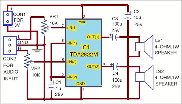
A simplified circuit diagram for such audio amplifier is shown below. The circuit consists of all necessary components for the amplifier requirement with this chip. The component count is so less that anyone having little experience with electronics can create such amplifier circuit.

Here is image for TDA2822M audio amplifier

In the above circuit all components like resistors, capacitors and variable volume controls are connected to different pins of the IC TDA2822M. There components are circuit requirements and they are used to control oscillations and positive feed back in the amplifier circuit. Such components are big in size and heavier so that they can't be constructed inside IC chip. Some chips known as hybrid contains such discrete components inside even. But as this IC chip is monolithic so components are located outside the chip.

Here in this circuit the audio input is provide to pin 6 and pin 7 trough volume controls or variable resistances which acts like atenuators for the audio signal and use to control the gain of the amplifier. Most of the time single shaft stereo type volume control is used in which there are two volume controls are constructed and a single shaft varies both volume controls. Out put to 4 Ohm speakers is provided through two 100UF 25V capacitors. They are AC coupling capacitors and avoid any DC to the speakers from the amplifier. The two inverting input pins pin 5 and 8 are connected together and they are connected to ground through a 1UF 25V electrolytic capacitor to avoid any positive feed back or oscillation in the circuit. At pin 2 of the IC 3V power supply positive is connected which is decoupled with a 10UF 25V capacitor. This capacitor should be located as close as possible to the chip to avoid harmonics and provide good filtration to the power line. Ground or negative terminal of the power is connected at pin 4 to the IC chip.

This circuit has an overall good performance but it is off course and old style class AB amplifier design on chip. New designs uses class D amplifier with great efficiency and less power consumption from battery. Such class D amplifiers is a new technology and are becoming popular in new audio designs for last few years. They are producing much less heat and their heat sink requirement is less and small heat sinks can even do for such amplifiers.

PCB layout for TDA2822M

Here is the copper pattern for the pcb for this project. If you are going to do this project, this pcb pattern will help you a lot. This is especially important for university students. The following pcb layout will help identify components locations. The pcb layout is silk printed for this project. The silk print carries all necessary information regarding the whole circuit and project.


Continue reading

Smoke detector circuit

 A smoke detector circuit is one which is used to detect un-burned fuel smoke created due to burning process. Such circuits are useful for building safety and house hold safety requirements. Such circuits are compulsory in some countries to be installed in the buildings if you are going to build new building or house. Without such alarm circuit installation, the authorities would not pass your building and will now allow residents to live in such building due to fire hazards and lake of fire safety.


There are many kind of fire alarm circuit available in the market. Some uses special sensors and detectors to perform the job. Whereas some uses very basic sensors for such kind of job. The below circuit is also using a very basic concept and very basic circuit design for the purpose. It uses an LED and an LDR to detect smoke passing between both of them. This a must for this circuit to fix it in the path of smoke to pass the smoke between the led and ldr. Otherwise if smoke is not passing between led and lrd the circuit wouldn't detect the smoke and would not alarm in case of fire or smoke. Such circuit have a beauty that it is very simple and very low price and also is consuming very low power from the power supply or from the battery. There are some other kind of sensors available in the market which are a bit expensive and also they are consuming too much power form the power source. Such circuits details article would also be available here on this blog.


Smoke detector circuit using basic sensors and components

In the above circuit when smoke is passed between led and ldr, the ldr resistance changes due to change in the light intensity passes through the smoke. The ldr resistance decreases with more smoke. The would decrease the base current of the transistor. The transistor is connected here in this circuit in common collector configuration. Then the output of this transistor is fed to the cob IC which is a pre amplifier for the small signal received from the transistor. The first VR which is 100K in value under the ldr is used to calibrate the circuit. The output of the cob ic is fet to the ic2 which is a power amplifier and is TDA2002 though another VR which is also of 100K value. The output of the power amplifire IC TDA2002 is fed to the loud speaker which is of 8R impedance through a capacitor which is of 1000u and 25v value. The rest of the components resistance and capacitors are making filter network for the output of the audio power output IC TDA2002. The circuit is powered up from a 9V battery or a 9V PP3 battery. Power supply is off course better because battery would drain up with the passage of time. The other way is to use a rechargeable battery with appropriate charging arrangement to make the circuit battery powered and also free of battery replacement tension.


Continue reading

Industrial motors

Industrial motors
Motors are very commonly used in industry. Motors are the work horses in industry. They are every where in industry and running different kind of loads in everyday life. They run fans, pumps, compressors, blowers, belt conveyors, elevators, spinners, rollers, mills, transmissions, agitators, vibrators, apron conveyors, kilns and spinners etc.

There are many kinds of motors. Among them 98% cases ac induction motors are used. There are two further kinds of induction motors. First and the most commonly used one is squirrel cage induction motor and the second one is off course wound rotor or slip ring induction motor. The squirrel cage induction motor is the most used on in industry from a fraction of Kw to a few Mw power rating. The other type wound rotor or slip ring induction motor is used to drive very high torque load and have ability to start very slowly under very high torque load and controls its current by resistance addition in the rotor circuit. The rotor circuit impedance is controlling the stater supplied current by transformer action. So the way to control the stater current is to insert impedance in the rotor circuit. For this purpose slip rings are used to bring the rotor power out of the motor on carbon brushes to outside circuit where impedance is introduced to limit the current in the motor starting condition. Latter on such impedance is reduced to zero or short circuit is created on the rotor circuit to insure maximum current flow through the rotor circuit hence maximum torque from the motor. Such motors are used to drive high inertia loads. Such loads examples are mills, gearboxes and huge fans.

There is another kind of ac motor used rarely in industry is synchronous motor. Synchronous motor is rarely used due to its complex construction and difficult starting procedure. Such motor have its special benefits which makes it unique for special purpose use. Those benefits are very high torque and this motor can run any power factor value. It acts like a synchronous capacitor. Meaning to say it is correcting the system power factor also if installed in industry. Also the other benefit is of-course running some mechanical load along with power factor correction.

There are DC motors used too in industry and in house hold use. In industry in older days such dc motors were very commonly used due their powerful torque and due to there speed control characteristics. As in older days frequency inversters or vfd were not invented to vary the induction motor, so DC motor was the only solution to achieve variable speed control.
Continue reading